
Search

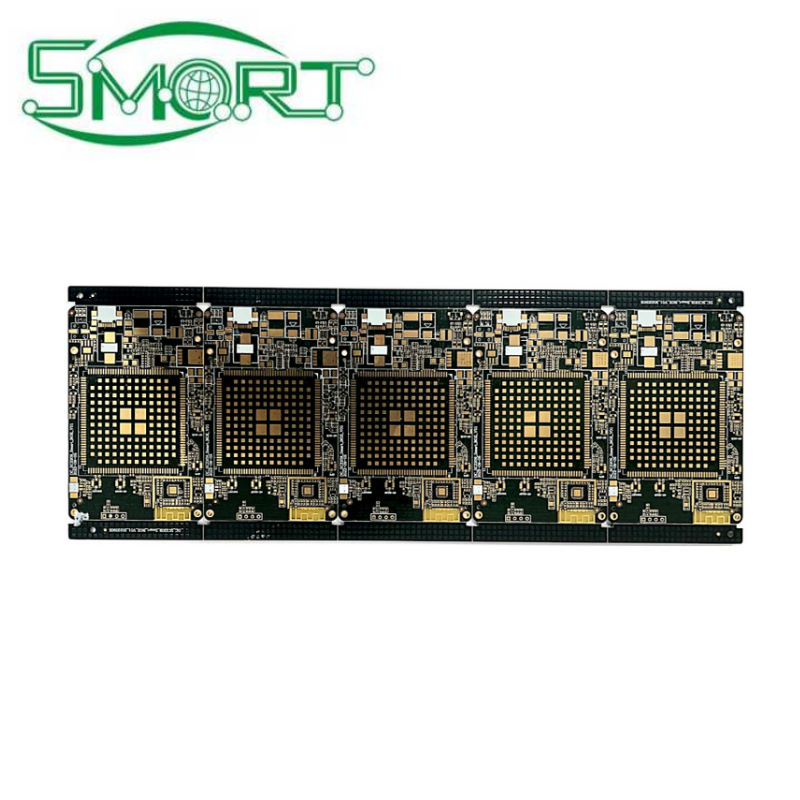
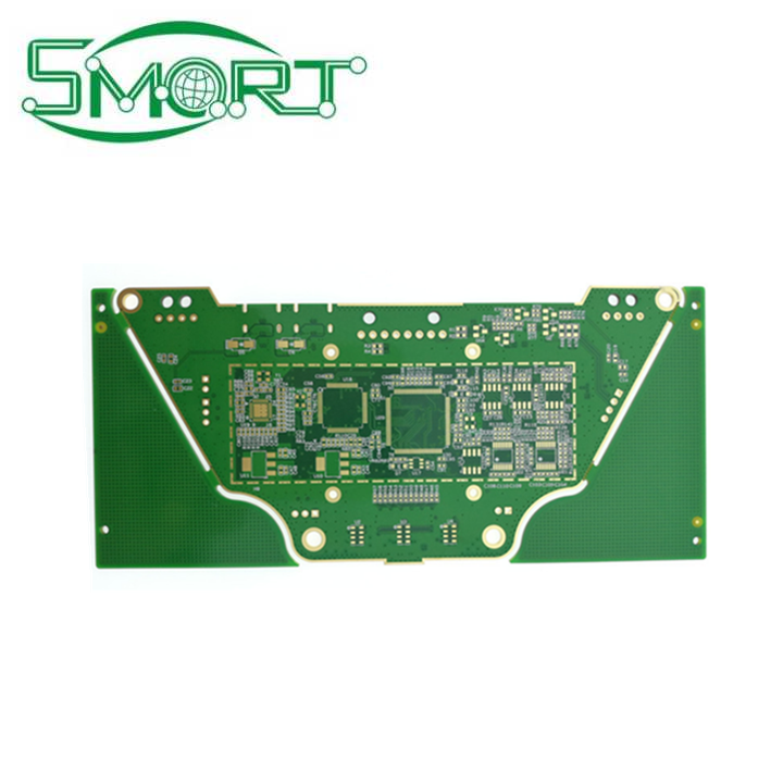
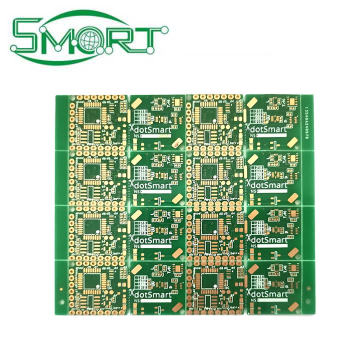
Heavy Copper 4oz PCB thick copper electronic circuit board industrial automation PCB circuit board other PCB
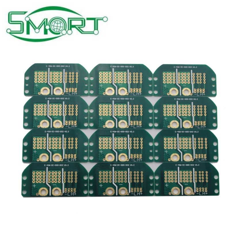
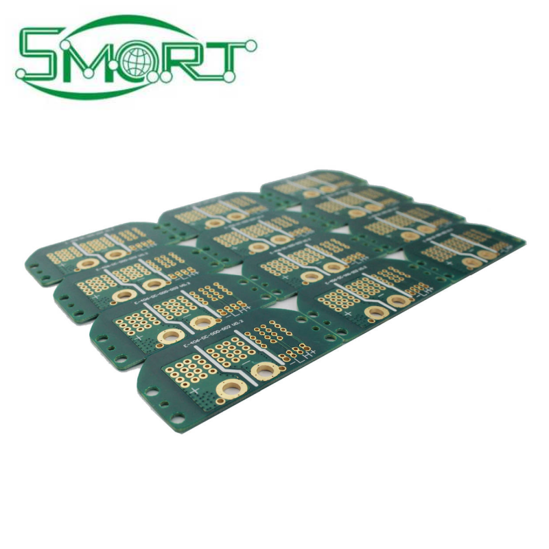
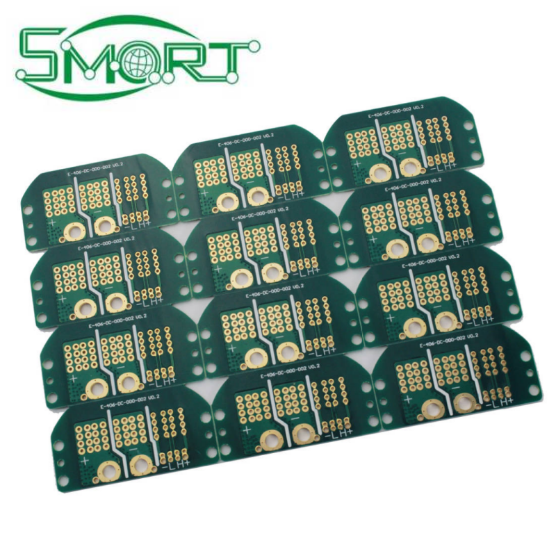
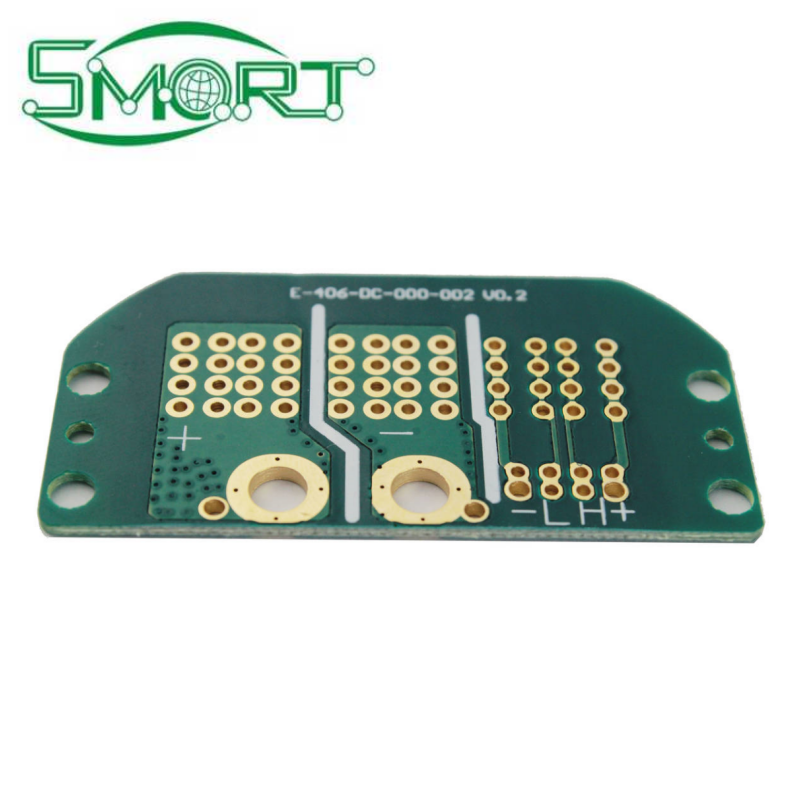
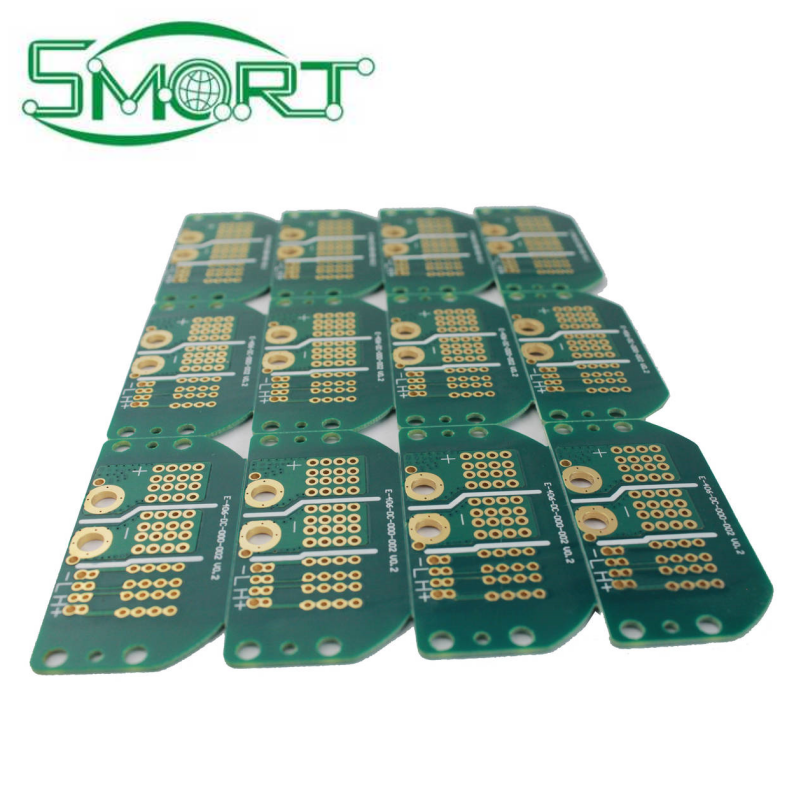
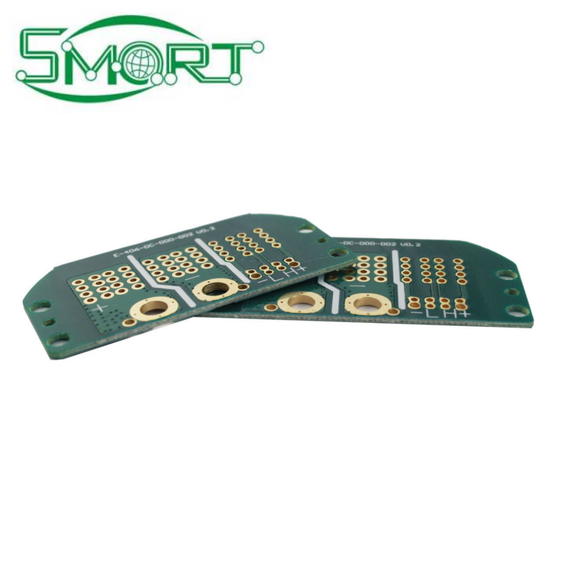
Heavy Copper 4oz PCB thick copper electronic circuit board industrial automation PCB circuit board other PCB
shared:


Q1.What is needed for quotation?
A1: PCB : Quantity, Gerber file and Technic requirements(material,surface finish treatment, copper thickness,board thickness ,...)PCBA: PCB information, BOM, (Testing documents...)
A1: PCB : Quantity, Gerber file and Technic requirements(material,surface finish treatment, copper thickness,board thickness ,...)PCBA: PCB information, BOM, (Testing documents...)
Q2: MOQ?
A2: There is no MOQ in Smart.We are able to handle Small as well as large volume production with flexibility.
A2: There is no MOQ in Smart.We are able to handle Small as well as large volume production with flexibility.
Q3: Which type of PCBs do you expert in?
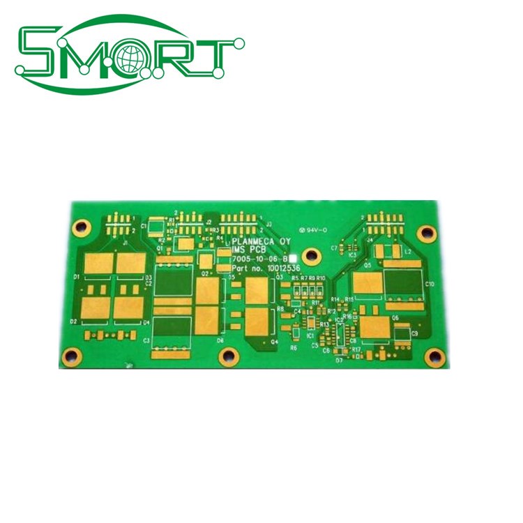
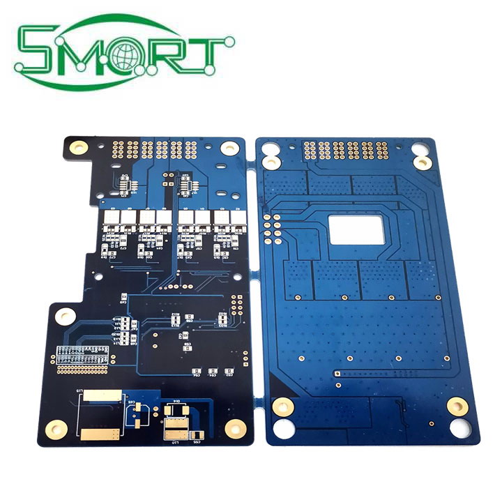
A3: We are specialized in producing Singe-side PCB,Double-side PCB, Multilayer PCB,Aluminium PCB,Spray Tin PCB,Immersed Gold PCB, etc.
Q4: What is your Lead time?
A4: Lead time is usually punctual here, usually 5-10 days for PCB sample, 10-15 days for mass production. For some special situation,we can also advise customer in advance to avoid any inexpectation or loss at customer side.
Q5: I only have the pcb sample, not pcb file, can you produce it for me?
A5: Yes, we can copy file based on your sample, this file names gerber, and production then is accorded to gerber file.
Q6: What is your testing policy and how you controle the quality?
A6: For sample, usually tested by flying probe; for PCB Volume over 3 square meters, usually tested by fixture, this will be more faster. Due to there’s many steps to PCB production, we usually do inspection after every step.
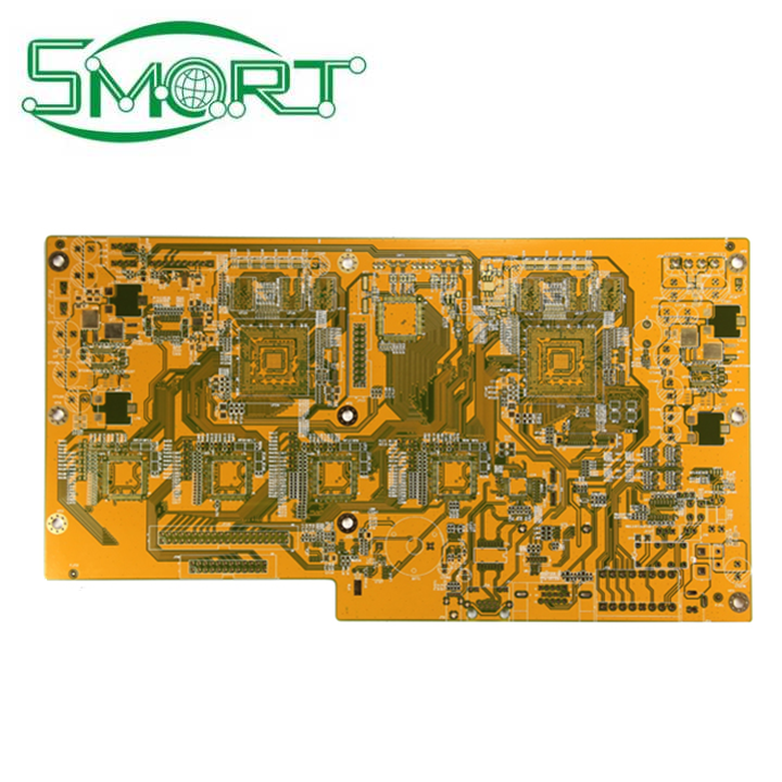
Q7: Will you allow me to put several part number together into one panel?
A7: Yes, this is usually happen in we factory, this way can help customers reduce some cost and to a certain degree, it can help reduce some assembly cost.
Q8: Will my file be safe after you get it ?
A6: For sample, usually tested by flying probe; for PCB Volume over 3 square meters, usually tested by fixture, this will be more faster. Due to there’s many steps to PCB production, we usually do inspection after every step.
Q7: Will you allow me to put several part number together into one panel?
A7: Yes, this is usually happen in we factory, this way can help customers reduce some cost and to a certain degree, it can help reduce some assembly cost.
Q8: Will my file be safe after you get it ?
A8: Yes , we will not release your design to third party unless with your permission .And we can signthe NDA before you send the file.
Q9: Do you accept process materials supplied by clients?
A9: Yes, we can provide component source, and we also accept component from client
A9: Yes, we can provide component source, and we also accept component from client
Q10: PCB shipment?
A10: This is depend on customer, sometimes we ship through our forwarder, who is also the agency of DHL, TNT, UPS, Fedex, and so on.Our forwarder can provide too much better freight cost than we get directly from those express enterprise.
Q11: Shipping cost?
A11: The shipping cost is determined by the destination, weight, packing size of the goods. Please let us know if you need us to quote you the shipping cost.


CONTACT INFO Shenzhen Smart Electronics Co., Ltd
|
|


Copyright © 2021 Shenzhen Smart Electronics Co., Ltd All rights reserved